


Request Quote
(Ships tomorrow)
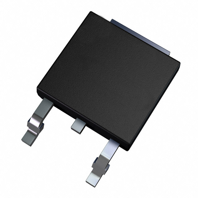
FDD3670 N-Channel MOSFET 100V 34A Equivalent & Substitute Parts
Part Overview
The FDD3670 is an N-Channel MOSFET manufactured by onsemi, rated for 100V drain-to-source voltage with 34A continuous drain current at 25°C. The device is housed in a TO-252AA surface mount package and belongs to the PowerTrench® series. The FDD3670 maintains Active product status with full RoHS3 compliance and unlimited moisture sensitivity level (MSL 1).
Substitute parts are necessary when the FDD3670 reaches end-of-life status, when inventory constraints occur, or when design requirements necessitate alternative electrical or thermal characteristics within the same voltage and current class.
Substiute Parts
Key Parameters
| Parameter | FDD3670 Specification |
|---|---|
| Drain-to-Source Voltage (Vdss) | 100 V |
| Continuous Drain Current (Id) @ 25°C | 34 A (Ta) |
| On-State Resistance (Rds On) @ Id, Vgs | 32 mOhm @ 7.3A, 10V |
| Gate Threshold Voltage (Vgs(th)) @ Id | 4 V @ 250 µA |
| Gate Charge (Qg) @ Vgs | 80 nC @ 10 V |
| Input Capacitance (Ciss) @ Vds | 2490 pF @ 50 V |
| Power Dissipation (Max) | 3.8 W (Ta), 83 W (Tc) |
| Operating Temperature Range | -55°C to 175°C (TJ) |
| Package Type | TO-252-3, DPAK (2 Leads + Tab), SC-63 |
| Mounting Type | Surface Mount |
| RoHS Status | ROHS3 Compliant |
| Moisture Sensitivity Level | 1 (Unlimited) |
Substitute Part Grouping Explanation
Substitution eligibility for the FDD3670 is determined by the following critical parameters:
Mandatory Matching Parameters:
- Drain-to-Source Voltage (Vdss): 100 V
- Package Type: TO-252-3, DPAK (2 Leads + Tab), SC-63
- Mounting Type: Surface Mount
- Operating Temperature Range: -55°C to 175°C minimum
Allowable Variation Parameters:
- Continuous Drain Current (Id): Equal to or greater than 34 A
- On-State Resistance (Rds On): Equal to or lower than 32 mOhm (lower resistance indicates improved performance)
- Gate Charge (Qg): Lower values reduce switching losses
- Power Dissipation: Higher thermal capability indicates improved performance margin
- Gate Threshold Voltage (Vgs(th)): Within ±20V gate voltage specification
- Input Capacitance (Ciss): Variation acceptable within switching frequency constraints
Substitute parts must maintain N-Channel MOSFET technology with Metal Oxide construction and support the same gate voltage range (±20V maximum).
Parameter Comparison
| Parameter | FDD3670 | BUK7227-100B,118 | BUK7240-100A,118 | IPD30N10S3L34ATMA1 | STD25N10F7 | STD25NF10LT4 | STD25NF10T4 | STD40NF10 | SUD35N10-26P-E3 |
|---|---|---|---|---|---|---|---|---|---|
| Vdss (V) | 100 | 100 | 100 | 100 | 100 | 100 | 100 | 100 | 100 |
| Id @ 25°C (A) | 34 (Ta) | 48 (Tc) | 34 (Tc) | 30 (Tc) | 25 (Tc) | 25 (Tc) | 25 (Tc) | 50 (Tc) | 35 (Tc) |
| Rds On (mOhm) @ Id, Vgs | 32 @ 7.3A, 10V | 27 @ 25A, 10V | 40 @ 25A, 10V | 31 @ 30A, 10V | 35 @ 12.5A, 10V | 35 @ 12.5A, 10V | 38 @ 12.5A, 10V | 28 @ 25A, 10V | 26 @ 12A, 10V |
| Vgs(th) (V) @ Id | 4 @ 250 µA | 4 @ 1 mA | 4 @ 1 mA | 2.4 @ 29 µA | 4.5 @ 250 µA | 2.5 @ 250 µA | 4 @ 250 µA | 4 @ 250 µA | 4.4 @ 250 µA |
| Qg (nC) @ Vgs | 80 @ 10V | 37 @ 10V | Not specified | 31 @ 10V | 14 @ 10V | 52 @ 5V | 55 @ 10V | 62 @ 10V | 47 @ 10V |
| Ciss (pF) @ Vds | 2490 @ 50V | 2789 @ 25V | 2293 @ 25V | 1976 @ 25V | 920 @ 50V | 1710 @ 25V | 1550 @ 25V | 2180 @ 25V | 2000 @ 12V |
| Power Dissipation (W) | 3.8 (Ta), 83 (Tc) | 167 (Tc) | 114 (Tc) | 57 (Tc) | 40 (Tc) | 100 (Tc) | 100 (Tc) | 125 (Tc) | 8.3 (Ta), 83 (Tc) |
| Operating Temp (°C) | -55 to 175 | -55 to 185 | -55 to 175 | -55 to 175 | -55 to 175 | -55 to 175 | -55 to 175 | -55 to 175 | -55 to 175 |
| Package | TO-252AA | DPAK | DPAK | PG-TO252-3-11 | DPAK | DPAK | DPAK | DPAK | TO-252AA |
| Product Status | Active | Obsolete | Obsolete | Active | Active | Active | Active | Active | Active |
| RoHS Status | ROHS3 | ROHS3 | ROHS3 | ROHS3 | ROHS3 | ROHS3 | ROHS3 | ROHS3 | ROHS3 |
Engineering Selection Recommendations
Primary Substitutes (Active Status, Direct Replacement):
SUD35N10-26P-E3 (Vishay Siliconix) is the preferred direct substitute. It matches the FDD3670 in voltage rating (100V), package type (TO-252AA), and thermal dissipation (83W Tc). The continuous drain current is 35A, exceeding the FDD3670 specification of 34A. On-state resistance is 26 mOhm at 12A/10V, providing superior performance. Gate charge is 47 nC, lower than the FDD3670 at 80 nC, reducing switching losses. Operating temperature range matches at -55°C to 175°C. RoHS3 compliance is confirmed. REACH status is Affected, requiring verification for specific applications.
IPD30N10S3L34ATMA1 (Infineon Technologies) provides an alternative with matching voltage (100V) and package compatibility (PG-TO252-3-11). Continuous drain current is 30A, slightly below the FDD3670 at 34A. On-state resistance is 31 mOhm at 30A/10V, comparable to the FDD3670. Gate threshold voltage is 2.4V, lower than the FDD3670 at 4V, enabling faster switching response. Gate charge is 31 nC, significantly lower than the FDD3670, reducing switching losses. Power dissipation is 57W Tc. Product status is Active with RoHS3 compliance.
Secondary Substitutes (Active Status, Current Derating Required):
STD25NF10T4 (STMicroelectronics) is an Active product with 100V rating and DPAK package. Continuous drain current is 25A, requiring 26% current derating from the FDD3670 specification. On-state resistance is 38 mOhm at 12.5A/10V. Power dissipation is 100W Tc, providing thermal margin. Gate charge is 55 nC at 10V. This substitute is suitable for applications where the 25A current rating is sufficient.
STD25NF10LT4 (STMicroelectronics) is an Active product with 100V rating and DPAK package. Continuous drain current is 25A, requiring 26% current derating. On-state resistance is 35 mOhm at 12.5A/10V. Power dissipation is 100W Tc. Gate threshold voltage is 2.5V, lower than the FDD3670. This substitute provides improved switching characteristics with lower gate charge (52 nC at 5V).
STD40NF10 (STMicroelectronics) is an Active product with 100V rating and DPAK package. Continuous drain current is 50A, exceeding the FDD3670 specification by 47%. On-state resistance is 28 mOhm at 25A/10V, superior to the FDD3670. Power dissipation is 125W Tc. Gate charge is 62 nC at 10V. This substitute provides performance margin for high-current applications.
Obsolete Substitutes (Not Recommended for New Designs):
BUK7227-100B,118 (Nexperia USA Inc.) has Obsolete product status. Continuous drain current is 48A at Tc, exceeding the FDD3670. On-state resistance is 27 mOhm at 25A/10V. Power dissipation is 167W Tc. Operating temperature extends to 185°C. AEC-Q101 automotive qualification is provided. Obsolete status restricts use to legacy system maintenance only.
BUK7240-100A,118 (Nexperia USA Inc.) has Obsolete product status. Continuous drain current is 34A at Tc, matching the FDD3670 specification. On-state resistance is 40 mOhm at 25A/10V, higher than the FDD3670. Power dissipation is 114W Tc. AEC-Q101 automotive qualification is provided. Obsolete status restricts use to legacy system maintenance only.
Frequently Asked Questions (FAQ)
Q: Can the FDD3670 be replaced with a lower current-rated device?
A: No. Substitute devices must have continuous drain current equal to or greater than 34A to maintain circuit performance and thermal stability. Devices rated below 34A require circuit redesign and thermal analysis.
Q: What is the significance of the TO-252AA package designation?
A: The TO-252AA package is a surface mount DPAK variant with specific lead geometry and thermal characteristics. Substitutes must use compatible package types (TO-252-3, DPAK, SC-63) to ensure PCB footprint compatibility and thermal performance equivalence.
Q: How does on-state resistance (Rds On) affect substitution?
A: Lower Rds On values reduce power dissipation and heat generation. Substitutes with Rds On equal to or lower than 32 mOhm at the specified current and gate voltage provide equivalent or improved performance. Higher Rds On values increase power loss and require thermal margin verification.
Q: Why is gate charge (Qg) important for substitution?
A: Gate charge determines switching speed and driver circuit requirements. Lower gate charge reduces switching losses and allows faster switching frequencies. The FDD3670 has 80 nC at 10V; substitutes with lower gate charge improve efficiency but require driver compatibility verification.
Q: Are obsolete parts acceptable for new designs?
A: No. Obsolete parts (BUK7227-100B,118 and BUK7240-100A,118) are restricted to legacy system maintenance and repair only. New designs must use Active status devices to ensure long-term supply availability and manufacturing consistency.
Q: What does RoHS3 compliance mean for substitution?
A: RoHS3 compliance indicates the device meets Restriction of Hazardous Substances Directive requirements. All listed substitutes maintain RoHS3 compliance, ensuring regulatory equivalence for applications subject to RoHS requirements.
Q: How does operating temperature range affect substitution?
A: The FDD3670 operates from -55°C to 175°C. Substitutes must support this range minimum. BUK7227-100B,118 extends to 185°C, providing additional thermal margin. Devices with lower maximum temperature ratings are not acceptable.
Q: What is the difference between Ta and Tc current ratings?
A: Ta (ambient temperature) current rating is measured at 25°C ambient with natural convection. Tc (case temperature) current rating is measured at 25°C case temperature with controlled thermal conditions. The FDD3670 specifies 34A at Ta; substitutes specify current at Tc, requiring thermal analysis for direct comparison.
Q: Can the IPD30N10S3L34ATMA1 replace the FDD3670 despite lower current rating?
A: The IPD30N10S3L34ATMA1 has 30A continuous drain current, 4A below the FDD3670 specification. Substitution is acceptable only if circuit analysis confirms that peak and continuous current demands do not exceed 30A. Thermal margin and switching characteristics are superior, but current derating is mandatory.
Q: Why is SUD35N10-26P-E3 listed as the preferred substitute?
A: SUD35N10-26P-E3 matches the FDD3670 in voltage (100V), package (TO-252AA), thermal dissipation (83W Tc), and operating temperature range (-55°C to 175°C). Continuous drain current is 35A, exceeding the 34A specification. On-state resistance is 26 mOhm, superior to the FDD3670 at 32 mOhm. Gate charge is 47 nC, reducing switching losses. Active product status ensures supply continuity.
Alternative Parts

SJ6012L2TP
Littelfuse Inc.
6 Alternative Parts

JMK107BBJ476MA-RE
Taiyo Yuden
10 Alternative Parts

GMK107BBJ475MA-T
Taiyo Yuden
5 Alternative Parts
SJ6020N2ARP
Littelfuse Inc.
3 Alternative Parts
SJ6025R2ATP
Littelfuse Inc.
4 Alternative Parts

2474-05L
API Delevan Inc.
1 Alternative Parts

4590R-684K
API Delevan Inc.
1 Alternative Parts

CM6560R-334
API Delevan Inc.
1 Alternative Parts

CM6460-104
API Delevan Inc.
1 Alternative Parts

5526-12
API Delevan Inc.
1 Alternative Parts