


Request Quote
(Ships tomorrow)
CDCVF857ZQLR Equivalent & Substitute Parts
Part Overview
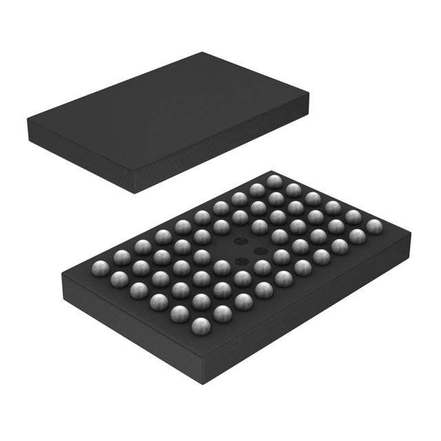
The CDCVF857ZQLR is a PLL Clock Driver IC manufactured by Texas Instruments, designed for high-speed clock distribution applications with a maximum frequency of 220MHz. This device features SSTL-2 input and output signaling, operates at 2.3V to 2.7V supply voltage, and is housed in a 56-VFBGA package. The product is currently classified as obsolete, necessitating identification of functionally equivalent alternatives for ongoing system support and new designs requiring similar clock distribution capabilities.
Substiute Parts
Key Parameters
| Parameter | Value |
|---|---|
| Manufacturer Part Number | CDCVF857ZQLR |
| Manufacturer | Texas Instruments |
| Category | Clock/Timing |
| Description | IC PLL CLOCK DRIVER 56BGA |
| Type | PLL Clock Driver |
| Frequency - Max | 220MHz |
| Input Signaling | SSTL-2 |
| Output Signaling | SSTL-2 |
| Voltage - Supply | 2.3V ~ 2.7V |
| Operating Temperature | -40°C ~ 85°C |
| Package / Case | 56-VFBGA |
| Product Status | Obsolete |
| RoHS Status | ROHS3 Compliant |
Substitute Part Grouping Explanation
Substitution of the CDCVF857ZQLR is determined by the following critical parameters:
- Frequency Capability: Maximum operating frequency must meet or exceed 220MHz
- Supply Voltage Compatibility: Operating voltage range must encompass 2.3V to 2.7V
- Output Signaling: SSTL-2 output is required for direct interface compatibility
- Package Compatibility: 56-pin BGA package variants (VFBGA, TFBGA, CABGA) with equivalent pinout and footprint dimensions
- Number of Circuits: Single circuit configuration
- Compliance Standards: ROHS3 compliance and EAR99 classification maintained
The substitute part 95V2F857AHLFT from Renesas Electronics Corporation meets these substitution criteria with equivalent electrical performance and package compatibility.
Parameter Comparison
| Parameter | CDCVF857ZQLR (Main Part) | 95V2F857AHLFT (Substitute) |
|---|---|---|
| Manufacturer | Texas Instruments | Renesas Electronics Corporation |
| Category | Clock/Timing | Clock/Timing |
| Type | PLL Clock Driver | Memory DDR Clock Buffer/Driver |
| Frequency - Max | 220MHz | 233MHz |
| Input Signaling | SSTL-2 | LVCMOS |
| Output Signaling | SSTL-2 | SSTL-2 |
| Voltage - Supply | 2.3V ~ 2.7V | 2.3V ~ 2.7V |
| Operating Temperature | -40°C ~ 85°C | 0°C ~ 85°C |
| Package / Case | 56-VFBGA | 56-TFBGA |
| Supplier Device Package | 56-BGA Microstar Junior (7x4.5) | 56-CABGA (4.5x7.0) |
| Number of Circuits | 1 | 1 |
| Product Status | Obsolete | Active |
| RoHS Status | ROHS3 Compliant | ROHS3 Compliant |
| Moisture Sensitivity Level (MSL) | 2 (1 Year) | 1 (Unlimited) |
Engineering Selection Recommendations
The 95V2F857AHLFT serves as a direct functional substitute for the obsolete CDCVF857ZQLR based on the following engineering criteria:
Electrical Compatibility: Both devices operate within the identical 2.3V to 2.7V supply voltage range. The substitute part exceeds the frequency requirement with 233MHz maximum capability versus the original 220MHz specification. SSTL-2 output signaling is maintained for seamless interface compatibility.
Package Compatibility: Both devices utilize 56-pin BGA packages with equivalent footprint dimensions (7x4.5mm and 4.5x7.0mm respectively), enabling direct PCB layout substitution without redesign.
Compliance and Availability: The substitute part maintains ROHS3 compliance and EAR99 classification consistent with the original device. Active product status ensures long-term availability and supply chain continuity, addressing the obsolescence of the original part.
Operational Considerations: The substitute part operates across a narrower temperature range (0°C to 85°C versus -40°C to 85°C). Applications requiring extended low-temperature operation below 0°C must retain the original part or implement thermal management strategies. The substitute part features superior moisture sensitivity characteristics (MSL 1 versus MSL 2), providing enhanced reliability in humid storage and operational environments.
Frequently Asked Questions (FAQ)
Q: Can the 95V2F857AHLFT directly replace the CDCVF857ZQLR without PCB modifications?
A: The 56-pin BGA packages are mechanically compatible with equivalent footprint dimensions. However, verify pinout compatibility with device datasheets before implementation, as input signaling differs (LVCMOS versus SSTL-2 input on the original).
Q: What is the primary difference in input signaling between these devices?
A: The CDCVF857ZQLR accepts SSTL-2 input signaling, while the 95V2F857AHLFT accepts LVCMOS input signaling. Both devices output SSTL-2 signals. Ensure your clock source provides the appropriate input signal type for the selected device.
Q: Is the substitute part suitable for applications requiring -40°C operation?
A: No. The 95V2F857AHLFT operates from 0°C to 85°C, making it unsuitable for applications requiring extended low-temperature operation below 0°C. Evaluate alternative substitutes or retain the original part for such applications.
Q: What is the significance of the different MSL ratings?
A: The substitute part carries MSL 1 (unlimited shelf life) compared to MSL 2 (1-year shelf life) for the original. This indicates superior moisture resistance and reduced risk of moisture-induced failures during storage and handling.
Q: Are both devices RoHS compliant?
A: Yes. Both the CDCVF857ZQLR and 95V2F857AHLFT are ROHS3 compliant and maintain EAR99 export classification.
Alternative Parts

SJ6012L2TP
Littelfuse Inc.
6 Alternative Parts

JMK107BBJ476MA-RE
Taiyo Yuden
10 Alternative Parts

GMK107BBJ475MA-T
Taiyo Yuden
5 Alternative Parts
SJ6020N2ARP
Littelfuse Inc.
3 Alternative Parts
SJ6025R2ATP
Littelfuse Inc.
4 Alternative Parts

2474-05L
API Delevan Inc.
1 Alternative Parts

4590R-684K
API Delevan Inc.
1 Alternative Parts

CM6560R-334
API Delevan Inc.
1 Alternative Parts

CM6460-104
API Delevan Inc.
1 Alternative Parts

5526-12
API Delevan Inc.
1 Alternative Parts