


Request Quote
(Ships tomorrow)
CD4013BCN Equivalent & Substitute Parts
Part Overview
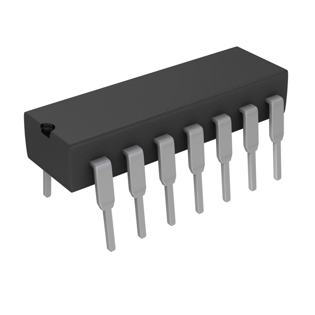
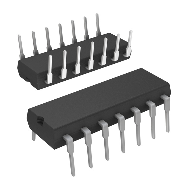
The CD4013BCN is a dual D-type flip-flop logic integrated circuit manufactured by onsemi, housed in a 14-DIP package. This device implements two independent D-type flip-flops with Set (Preset) and Reset functions, operating across a wide supply voltage range of 3V to 15V. The CD4013BCN is classified as obsolete, making identification of equivalent and substitute parts essential for design continuity and procurement planning. Active alternatives from other manufacturers provide functional equivalence while offering improved availability and compliance status.
Substiute Parts
Key Parameters
| Parameter | Value |
|---|---|
| Part Number | CD4013BCN |
| Manufacturer | onsemi |
| Category | Logic |
| Type | D-Type Flip-Flop |
| Number of Elements | 2 |
| Number of Bits per Element | 1 |
| Output Type | Complementary |
| Clock Frequency | 15.5 MHz |
| Max Propagation Delay @ 15V, 50pF | 120 ns |
| Trigger Type | Positive Edge |
| Voltage - Supply | 3V ~ 15V |
| Current - Output High, Low | 8.8 mA, 8.8 mA |
| Current - Quiescent (Iq) | 4 µA |
| Input Capacitance | 5 pF |
| Operating Temperature | -55°C ~ 125°C |
| Package / Case | 14-DIP (0.300", 7.62mm) |
| Mounting Type | Through Hole |
| Product Status | Obsolete |
Substitute Part Grouping Explanation
Substitution of the CD4013BCN is determined by strict adherence to the following electrical and mechanical parameters:
Core Compatibility Criteria:
- Dual D-type flip-flop architecture with 2 elements, 1 bit per element
- Complementary output configuration
- Positive edge trigger mechanism
- 14-DIP through-hole package (0.300", 7.62mm)
- Input capacitance of 5 pF
- Set (Preset) and Reset functionality
Allowable Parameter Variations:
- Clock frequency may exceed the original specification (higher performance acceptable)
- Propagation delay may be lower than the original specification (faster operation acceptable)
- Supply voltage range may be extended (wider range acceptable)
- Output current may be lower than the original specification (reduced drive capability acceptable within application limits)
- Quiescent current may vary within logic device norms
- Operating temperature range may be narrower than the original specification
Substitute Parts Identified:
- CD4013BE (Texas Instruments) – Direct manufacturer equivalent with active product status
- TC4013BP(N,F) (Toshiba Semiconductor and Storage) – Similar functional equivalent with active product status
Parameter Comparison
| Parameter | CD4013BCN (onsemi) | CD4013BE (Texas Instruments) | TC4013BP(N,F) (Toshiba) |
|---|---|---|---|
| Type | D-Type | D-Type | D-Type |
| Number of Elements | 2 | 2 | 2 |
| Number of Bits per Element | 1 | 1 | 1 |
| Output Type | Complementary | Complementary | Complementary |
| Clock Frequency | 15.5 MHz | 24 MHz | 20 MHz |
| Max Propagation Delay @ 15V, 50pF | 120 ns | 90 ns | 90 ns |
| Trigger Type | Positive Edge | Positive Edge | Positive Edge |
| Voltage - Supply | 3V ~ 15V | 3V ~ 18V | 3V ~ 18V |
| Current - Output High, Low | 8.8 mA, 8.8 mA | 6.8 mA, 6.8 mA | 3.4 mA, 3.4 mA |
| Current - Quiescent (Iq) | 4 µA | 4 µA | 120 µA |
| Input Capacitance | 5 pF | 5 pF | 5 pF |
| Operating Temperature | -55°C ~ 125°C | -55°C ~ 125°C | -40°C ~ 85°C |
| Package / Case | 14-DIP (0.300", 7.62mm) | 14-DIP (0.300", 7.62mm) | 14-DIP (0.300", 7.62mm) |
| Mounting Type | Through Hole | Through Hole | Through Hole |
| Product Status | Obsolete | Active | Active |
| RoHS Status | Not specified | ROHS3 Compliant | ROHS3 Compliant |
Engineering Selection Recommendations
CD4013BE (Texas Instruments) is the primary direct equivalent. This part maintains identical electrical specifications to the CD4013BCN while offering active product status, ensuring long-term availability. The CD4013BE provides improved clock frequency (24 MHz vs. 15.5 MHz) and faster propagation delay (90 ns vs. 120 ns), representing enhanced performance. The extended supply voltage range (3V ~ 18V vs. 3V ~ 15V) provides additional design flexibility. ROHS3 compliance status supports modern manufacturing and environmental requirements. Inventory availability of 55,300 units ensures procurement reliability.
TC4013BP(N,F) (Toshiba Semiconductor and Storage) serves as a secondary equivalent for applications where Toshiba component qualification is required. This part maintains core functional compatibility with identical package and pin configuration. The TC4013BP(N,F) operates at 20 MHz clock frequency and delivers 90 ns propagation delay, meeting or exceeding the original specification. The extended supply voltage range (3V ~ 18V) provides design margin. ROHS3 compliance is confirmed. The narrower operating temperature range (-40°C ~ 85°C vs. -55°C ~ 125°C) requires verification against application requirements. Quiescent current of 120 µA (vs. 4 µA in the original) may impact low-power applications. Inventory availability of 3,126 units supports procurement needs.
Frequently Asked Questions (FAQ)
Q: Can CD4013BE directly replace CD4013BCN without circuit modification?
A: Yes. The CD4013BE maintains identical pin configuration, package type (14-DIP), and core electrical specifications. No circuit modification is required. The improved performance characteristics (higher clock frequency, faster propagation delay) are backward compatible with designs specified for the CD4013BCN.
Q: What are the key differences between CD4013BE and TC4013BP(N,F)?
A: Both parts provide functional equivalence to the CD4013BCN. The CD4013BE offers superior performance (24 MHz vs. 20 MHz clock frequency) and lower quiescent current (4 µA vs. 120 µA). The TC4013BP(N,F) operates within a narrower temperature range (-40°C ~ 85°C vs. -55°C ~ 125°C) and provides lower output current drive (3.4 mA vs. 6.8 mA). Selection depends on application temperature requirements and output drive specifications.
Q: Is the TC4013BP(N,F) suitable for applications requiring the full -55°C ~ 125°C temperature range?
A: No. The TC4013BP(N,F) operates only within -40°C ~ 85°C. Applications requiring the full -55°C ~ 125°C range must use the CD4013BE or verify that the narrower range meets specific application requirements.
Q: Are both substitute parts RoHS compliant?
A: Yes. Both CD4013BE and TC4013BP(N,F) carry ROHS3 compliance certification, meeting current environmental and manufacturing standards.
Q: What is the impact of lower output current in the TC4013BP(N,F)?
A: The TC4013BP(N,F) provides 3.4 mA output current (high and low) compared to 8.8 mA in the CD4013BCN and 6.8 mA in the CD4013BE. Applications requiring higher output drive capability should use the CD4013BE. Verify that the TC4013BP(N,F) output current meets specific load requirements before selection.
Q: Can these parts be used interchangeably in existing designs?
A: Yes, within the constraints of operating temperature range and output current requirements. The CD4013BE provides the highest compatibility with the original CD4013BCN specification. The TC4013BP(N,F) requires verification of temperature range and output drive capability for the specific application.
Alternative Parts

SJ6012L2TP
Littelfuse Inc.
6 Alternative Parts

JMK107BBJ476MA-RE
Taiyo Yuden
10 Alternative Parts

GMK107BBJ475MA-T
Taiyo Yuden
5 Alternative Parts
SJ6020N2ARP
Littelfuse Inc.
3 Alternative Parts
SJ6025R2ATP
Littelfuse Inc.
4 Alternative Parts

2474-05L
API Delevan Inc.
1 Alternative Parts

4590R-684K
API Delevan Inc.
1 Alternative Parts

CM6560R-334
API Delevan Inc.
1 Alternative Parts

CM6460-104
API Delevan Inc.
1 Alternative Parts

5526-12
API Delevan Inc.
1 Alternative Parts