


Request Quote
(Ships tomorrow)
Equivalent & Substitute Parts for 502MILFT Clock Generator IC
Part Overview
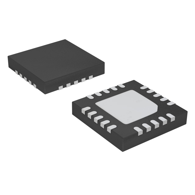
The 502MILFT is a Clock Generator IC manufactured by Renesas Electronics Corporation, designed for timing and clock distribution applications. This device operates at frequencies up to 140MHz and is housed in an 8-SOIC package. The product is currently classified as obsolete, making identification of functionally equivalent alternatives essential for design continuity and component procurement in legacy system maintenance and new designs requiring compatible timing solutions.
Substiute Parts
Key Parameters
| Parameter | Value |
|---|---|
| Manufacturer Part Number | 502MILFT |
| Manufacturer | Renesas Electronics Corporation |
| Category | Clock/Timing |
| Type | Clock Generator |
| Package / Case | 8-SOIC (0.154", 3.90mm Width) |
| Frequency - Max | 140MHz |
| Voltage - Supply | 3V ~ 5.5V |
| Operating Temperature | -40°C ~ 85°C |
| PLL | Yes |
| Input | Clock, Crystal |
| Output | CMOS |
| Number of Circuits | 1 |
| Mounting Type | Surface Mount |
| RoHS Status | ROHS3 Compliant |
| Product Status | Obsolete |
Substitute Part Grouping Explanation
Substitute parts for the 502MILFT are qualified based on the following critical parameters that determine functional compatibility:
Primary Compatibility Criteria:
- Package type: 8-SOIC (0.154", 3.90mm Width) for direct PCB footprint compatibility
- Supply voltage range: 3V ~ 5.5V for circuit integration without redesign
- Operating temperature range: -40°C ~ 85°C for environmental specification alignment
- PLL functionality: Required for clock generation and multiplication capability
- Input support: Clock and/or Crystal input capability
- Output type: CMOS or TTL output compatibility with downstream logic
- Mounting type: Surface Mount for manufacturing process consistency
Substitution Logic: The 502MILFT can be replaced by components that maintain identical or superior electrical and mechanical specifications within these parameters. Substitute parts may exceed the original frequency specification (140MHz maximum) while maintaining backward compatibility. Output type expansion (CMOS to CMOS/TTL) represents functional enhancement without degradation.
Parameter Comparison
| Parameter | 502MILFT (Main) | NB3N502DR2G | NB3N502DG | 5P35021B-000NDGI8 |
|---|---|---|---|---|
| Manufacturer | Renesas Electronics | onsemi | onsemi | Renesas Electronics |
| Type | Clock Generator | PLL Clock Multiplier | PLL Clock Multiplier | Clock Generator |
| Package / Case | 8-SOIC | 8-SOIC | 8-SOIC | 20QFN |
| Frequency - Max | 140MHz | 190MHz | 190MHz | Not Specified |
| Voltage - Supply | 3V ~ 5.5V | 3V ~ 5.5V | 3V ~ 5.5V | Not Specified |
| Operating Temperature | -40°C ~ 85°C | -40°C ~ 85°C | -40°C ~ 85°C | Not Specified |
| PLL | Yes | Yes with Bypass | Yes with Bypass | Not Specified |
| Input | Clock, Crystal | Clock, Crystal | Clock, Crystal | Not Specified |
| Output | CMOS | CMOS, TTL | CMOS, TTL | Not Specified |
| Mounting Type | Surface Mount | Surface Mount | Surface Mount | Surface Mount |
| RoHS Status | ROHS3 Compliant | ROHS3 Compliant | ROHS3 Compliant | Not Specified |
| Product Status | Obsolete | Active | Active | Active |
Engineering Selection Recommendations
NB3N502DR2G and NB3N502DG (onsemi): These PLL Clock Multiplier ICs provide direct functional replacement for the 502MILFT with identical 8-SOIC packaging and electrical specifications. Both devices maintain the 3V ~ 5.5V supply voltage range and -40°C ~ 85°C operating temperature window. The maximum frequency specification of 190MHz exceeds the original 140MHz requirement, ensuring compatibility with existing designs. Both parts are ROHS3 compliant and currently in active production status. The NB3N502DR2G is supplied in Tape & Reel packaging, while the NB3N502DG is supplied in Tube packaging. Selection between these variants depends on procurement and assembly requirements.
5P35021B-000NDGI8 (Renesas Electronics): This Clock Generator IC from the original manufacturer represents an alternative within the Renesas product line. The device is supplied in 20QFN packaging, which differs from the 8-SOIC footprint of the main part. This package change requires PCB layout modification and is suitable only for new designs or redesign scenarios where footprint flexibility exists. The part is currently in active production status and maintains REACH compliance. Detailed electrical specifications for this alternative are not provided in the available data.
Selection Basis:
- For direct PCB compatibility without layout modification: NB3N502DR2G or NB3N502DG
- For Renesas product line continuity with package redesign capability: 5P35021B-000NDGI8
- For high-volume procurement: NB3N502DR2G (Tape & Reel packaging, 2978 Pcs inventory)
Frequently Asked Questions (FAQ)
Q: Can NB3N502DR2G and NB3N502DG be used interchangeably with 502MILFT? A: Yes. Both onsemi parts maintain identical 8-SOIC packaging, supply voltage range (3V ~ 5.5V), and operating temperature specifications (-40°C ~ 85°C). The primary difference is packaging format: NB3N502DR2G is supplied in Tape & Reel, while NB3N502DG is supplied in Tube. PCB footprint compatibility is identical.
Q: What is the advantage of the 190MHz maximum frequency in substitute parts? A: The substitute parts (NB3N502DR2G and NB3N502DG) specify 190MHz maximum frequency compared to the original 140MHz. This higher specification ensures the parts can handle existing designs without frequency-related limitations and provides margin for future design iterations.
Q: Why does 5P35021B-000NDGI8 use a different package? A: The 5P35021B-000NDGI8 uses 20QFN packaging instead of 8-SOIC. This package change reflects different design architecture and feature set within the Renesas product portfolio. This alternative requires PCB redesign and is suitable for new development rather than direct replacement scenarios.
Q: Are all substitute parts RoHS compliant? A: NB3N502DR2G and NB3N502DG are ROHS3 compliant. Compliance status for 5P35021B-000NDGI8 is not specified in available documentation.
Q: What is the difference between PLL and PLL with Bypass? A: The substitute parts feature PLL with Bypass capability, providing additional operational flexibility compared to the original PLL-only design. Bypass mode allows the device to function as a clock buffer when PLL multiplication is not required, expanding application versatility.
Q: Can output type differences (CMOS vs. CMOS/TTL) affect compatibility? A: The substitute parts support both CMOS and TTL output types, while the original 502MILFT supports CMOS only. This represents functional enhancement. Existing designs using CMOS output remain fully compatible. TTL output capability is an additional feature not present in the original part.
Alternative Parts

SJ6012L2TP
Littelfuse Inc.
6 Alternative Parts

JMK107BBJ476MA-RE
Taiyo Yuden
10 Alternative Parts

GMK107BBJ475MA-T
Taiyo Yuden
5 Alternative Parts
SJ6020N2ARP
Littelfuse Inc.
3 Alternative Parts
SJ6025R2ATP
Littelfuse Inc.
4 Alternative Parts

2474-05L
API Delevan Inc.
1 Alternative Parts

4590R-684K
API Delevan Inc.
1 Alternative Parts

CM6560R-334
API Delevan Inc.
1 Alternative Parts

CM6460-104
API Delevan Inc.
1 Alternative Parts

5526-12
API Delevan Inc.
1 Alternative Parts