


Request Quote
(Ships tomorrow)
2N4416 JFET N-Channel Transistor Equivalent & Substitute Parts
Part Overview
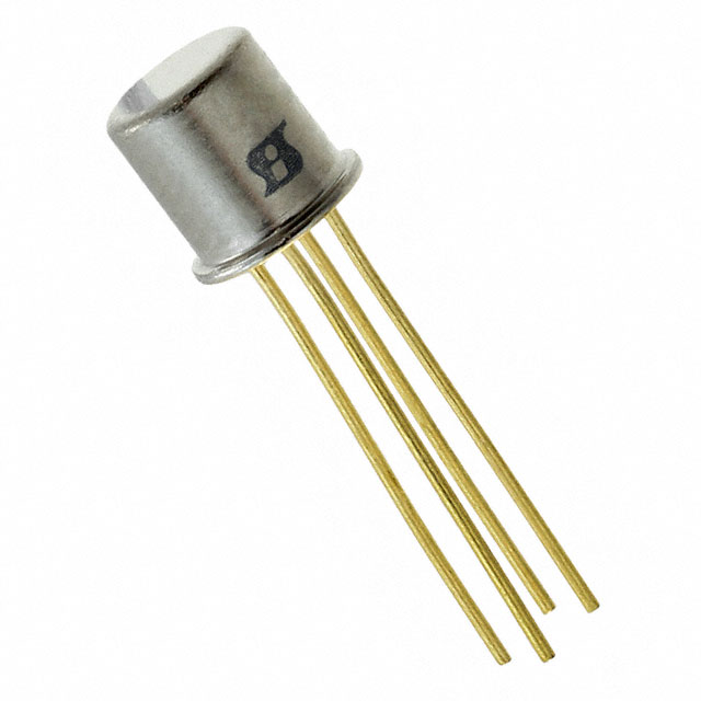
The 2N4416 is an N-Channel JFET transistor manufactured by Vishay Siliconix, designed for through-hole applications in the TO-206AF (TO-72) metal can package. This device operates at a maximum breakdown voltage of 30 V with a power dissipation rating of 300 mW and an operating temperature range of -50°C to 150°C. The 2N4416 is classified as obsolete, making identification of functionally equivalent alternatives necessary for ongoing design support and component procurement.
Substiute Parts
Key Parameters
| Parameter | Value | Condition |
|---|---|---|
| FET Type | N-Channel | — |
| Voltage - Breakdown (V(BR)GSS) | 30 V | — |
| Current - Drain (Idss) @ Vds | 5 mA | Vgs=0, @ 15 V |
| Voltage - Cutoff (VGS off) @ Id | 3 V | @ 1 nA |
| Input Capacitance (Ciss) (Max) | 4 pF | @ 15 V |
| Power - Max | 300 mW | — |
| Operating Temperature | -50°C to 150°C | TJ |
| Mounting Type | Through Hole | — |
| Package / Case | TO-206AF, TO-72-4 Metal Can | — |
| RoHS Status | RoHS non-compliant | — |
Substitute Part Grouping Explanation
The J111 (onsemi) qualifies as a functional substitute for the 2N4416 based on the following electrical and mechanical criteria:
Substitution-Determining Parameters:
- FET Type: Both devices are N-Channel JFETs
- Voltage - Breakdown (V(BR)GSS): J111 at 35 V exceeds the 2N4416 requirement of 30 V, providing margin
- Voltage - Cutoff (VGS off): Both specified at 3 V, ensuring gate threshold compatibility
- Mounting Type: Both are through-hole devices
- Operating Temperature Range: J111 range of -55°C to 150°C encompasses the 2N4416 range of -50°C to 150°C
- Power Dissipation: J111 at 625 mW exceeds the 2N4416 at 300 mW, providing thermal margin
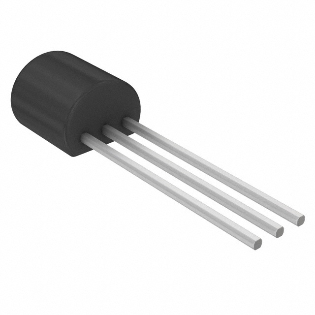
The J111 operates within the allowed electrical parameters for N-Channel JFET substitution and maintains through-hole mounting compatibility, though in a different package form factor (TO-92-3 versus TO-206AF).
Parameter Comparison
| Parameter | 2N4416 (Vishay Siliconix) | J111 (onsemi) | Notes |
|---|---|---|---|
| FET Type | N-Channel | N-Channel | Identical |
| Voltage - Breakdown (V(BR)GSS) | 30 V | 35 V | J111 provides 5 V margin |
| Current - Drain (Idss) @ Vds (Vgs=0) | 5 mA @ 15 V | 20 mA @ 15 V | J111 exhibits higher drain current |
| Voltage - Cutoff (VGS off) @ Id | 3 V @ 1 nA | 3 V @ 1 µA | Threshold voltage identical; measurement current differs |
| Power - Max | 300 mW | 625 mW | J111 provides greater thermal capacity |
| Operating Temperature | -50°C to 150°C | -55°C to 150°C | J111 range encompasses 2N4416 range |
| Mounting Type | Through Hole | Through Hole | Identical |
| Package / Case | TO-206AF (TO-72) | TO-226-3 (TO-92-3) | Different package; both through-hole |
| RoHS Status | RoHS non-compliant | ROHS3 Compliant | J111 meets modern compliance requirements |
Engineering Selection Recommendations
The J111 is suitable as a substitute for the 2N4416 in applications where the following conditions are met:
- The circuit design accommodates the TO-92-3 package footprint in place of the TO-206AF package
- The higher drain current characteristic (20 mA versus 5 mA at Vgs=0) is acceptable for the intended application
- The increased power dissipation capability (625 mW versus 300 mW) does not introduce unintended circuit behavior
- RoHS3 compliance of the J111 aligns with procurement and regulatory requirements
The J111 is an active product with substantial inventory availability (95,300 pcs), whereas the 2N4416 is obsolete. Selection of the J111 ensures long-term component availability and compliance with current environmental standards.
Frequently Asked Questions (FAQ)
Q: Can the J111 directly replace the 2N4416 in existing PCB designs?
A: Physical replacement requires PCB modification due to package differences. The 2N4416 uses TO-206AF (TO-72) metal can packaging, while the J111 uses TO-92-3 plastic packaging. Pin configurations differ, necessitating circuit board layout changes.
Q: What are the key electrical differences between these devices?
A: The J111 exhibits higher drain current (20 mA versus 5 mA at Vgs=0) and greater power dissipation capability (625 mW versus 300 mW). Both devices share identical gate cutoff voltage (3 V). The J111 provides higher breakdown voltage margin (35 V versus 30 V).
Q: Is the J111 suitable for low-signal applications originally designed for the 2N4416?
A: The higher Idss of the J111 may affect circuit biasing and gain characteristics in low-signal applications. Circuit analysis is required to confirm compatibility with the original design specifications.
Q: What compliance advantages does the J111 offer?
A: The J111 is ROHS3 compliant and an active product, whereas the 2N4416 is RoHS non-compliant and obsolete. The J111 ensures regulatory compliance and long-term availability for new designs and production continuity.
Q: Are there pin-to-pin compatibility considerations?
A: Both devices are N-Channel JFETs with gate, drain, and source terminals. However, physical pin arrangement and package form factor differ significantly. Mechanical and electrical verification is required for any substitution implementation.
Alternative Parts

SJ6012L2TP
Littelfuse Inc.
6 Alternative Parts

JMK107BBJ476MA-RE
Taiyo Yuden
10 Alternative Parts

GMK107BBJ475MA-T
Taiyo Yuden
5 Alternative Parts
SJ6020N2ARP
Littelfuse Inc.
3 Alternative Parts
SJ6025R2ATP
Littelfuse Inc.
4 Alternative Parts

2474-05L
API Delevan Inc.
1 Alternative Parts

4590R-684K
API Delevan Inc.
1 Alternative Parts

CM6560R-334
API Delevan Inc.
1 Alternative Parts

CM6460-104
API Delevan Inc.
1 Alternative Parts

5526-12
API Delevan Inc.
1 Alternative Parts